
with Improved Performance and Reliability
Vladimir Scarpa1 , Uwe Kirchner1, Rolf Gerlach², Ronny Kern1
nfineon Technologies
Siemenstrasse 2, 9500 Villach, Austria
² Am Campeon 1-12, 85579 Neubiberg, Germany
E-Mail: vladimir.scarpa@infineon.com
Abstract
This paper presents the new thinQ!™ 5th Generation (G5) of SiC Schottky diodes, from Infineon
Technologies. In G5, both the capacitive charge, Qc, and the forward voltage, V, have een
minimized through a new and exclusive production process. The improvements with
respect to previous Infineon thinQ!™ 2nd and 3rd Generation are discussed in this paper, with
the support of direct application tests results.
1. Introduction
Silicon carbide (SiC) schottky barrier diodes (SBDs) have been on the market since more
than a decade and sell today in millions of pieces per year, with proven quality in the field.
This confirms it as a mature technology, able to provide both full reliable and highperformance
ce devices [1]. Moreover, the increasing request for energy efficiency experienced
in the last years is at the base of the constantly growing observed in many applications. Besides high-end server and telecom SMPS, where SiC SBDs have become a standard, increasing
adoption is recorded mainly in solar inverters, motor drives and lighting.
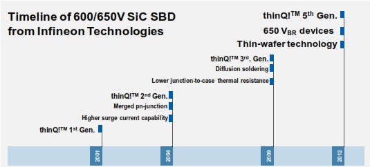
Fig. 1 summarizes the sequence of 600 V SiC SBD launched by Infineon Technologies.
Each new technology aimed to achieve a better price/performance ratio, thanks to new features,
translated into key benefits at application level.
In thinQ!TM2nd Generation (G2), a merged pn-junction has been integrated in the device
structure, in order to reduce the diode losses under high current conditions, enhancing thereforeore
the surge current capability of the devices [2].
Fig. 1. Timeline of SiC SBD generations of Infineon Technologies.
In thinQ!TM 3rd Generation (G3) has introduced a new solder technique, namely diffusion
soldering [3],resulting into an improved thermal conduction between the device chip and the
lead-frame. Main results are a lower junction-to-case thermal resistance Rh,JC, and consequent
high power dissipation per device area.
The newest thinQ!TM 5th Generation (G5) combines the above mentioned improvements of
former technologies with new features. The breakdown voltage has been increased to 650
V, while the devices are now produced with the exclusive thin-wafer technology [4], combined
with a compacter cell layout, which enable to obtain lower device capacitive charge.
The following sections will describe the main benefits brought by this technology and perform
a complete comparison among G5 and the former SiC diode technologies.
2. Technology Background
As extensively described in a previous publication [4], Infineon Technologies has developed
a manufacturing process able to reduce the wafer thickness down to ~1/3 of the original one,
as shown in Fig. 2 (a), without increasing the number of defects per unit area in the SiC wafer.
The thinning of the substrate results into a smaller differential resistance of the diode,
with a clear effect on the output characteristics of the device for the same unit area Fig. 2(b).
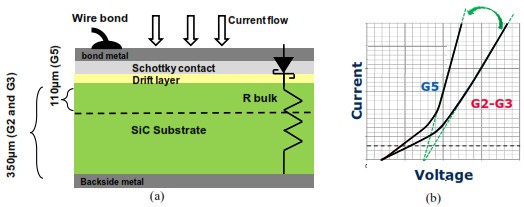
Fig. 2. (a)Schematic representation of a SIC diode (with thick and thin wafers). (b) forward characteristics of identical sized devices with thick (G2-G3) and thin(G5) substrates.
For a 650V SiC SBD, the substrate component is dominant in the overall diode resistance.
Thin-wafer technology enables thus a significant reduction of the diode differential resistance,
for identical chip sizes. This is graphically represented in the horizontal line in Fig. 2
(b), which indicates the forward characteristics of two the wafers with different substrate
thickness.
Together with the electrical characteristics, the thermal behaviour of the G5 chip is also improved.
A thinner chip results in a better thermal path between the wafer and the lead-frame.
As a consequence, identical power dissipation leads to a smaller junction temperature increase
in a G5 device compared to G2.
Fig. 3 shows the thermal simulation of two SiC SBD chips from two different technologies,
G2 and G5, in a TO-220 package, with the same power dissipation. Here one can see that,
for G5, the chip junction temperature is much lower due to improved thermal conduction to
the lead-frame. In addition, better heat spreading into the copper lead-frame is observed in
the G5 device.
At application level, the improved thermal behavior leads to higher surge current capability,
esp ecially for long current pulses, as it is shown in the next section.
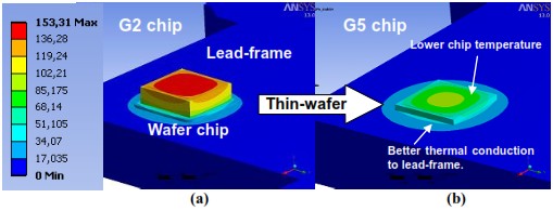
Fig. 3. Thermal behavior of SiC Diodes with equal sized chips but different thicknesses in a TO220 package, P = 75 W. Color scheme indicates the temperature, in °C. The backside of the
lead-frame is hold to constant temperature (0°C). (a) G2 device with thick chip thickness and soft soldering while (b) shows a thin chip with diffusion soldering.
3. Devices in G5
3.1. Tailoring of the Devices
Devices in G5 have been tailored to have forward voltage Vf=1.5 V under a given nominal
current and junction temperature Tj=25°C. Fig. 4 a) schematically shows
the positioning of the actual three families of SiC SBDs, with respect to Vf and Q– the total capacitive charge at a reverse voltage VRc =400V, – for the same nominal current. Fig. 4 (b) compares several current rated devices, from G2 and G5, where it is possible to see the massive reduction of the Qc (30-40%) in G5 devices.
By comparing G2 with G5, the total charge Qc is reduced despite same V, with consequent
lower switching losses, as indicated by the blue arrow. By comparing G2 with G3, instead,
G5 has comparable Qc but lower Vf, and consequently lower conductions losses, as again
indicated by the arrow.
As it will be demonstrated in section 4, the resulting performance of G5 is therefore always
better than that of the previous generations – for equally rated devices –from Infineon counterparts,over the entire power range.
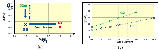
Fig. 4. (a) Device tailoring in G5, comparison with G2 and G3 regarding of Q
G2 . Arrows represent the benefit in terms of device lower losses. (b) Comparison of device Q between 5G and G2, for several current ratings.
3.2. Thermal resistance and surge current capability
With respect to device reliability of a power device, at least two other parameters are of
great importance, namely the thermal resistance between junction and case, Rth,jc, and the
surge current capability [5]. Therefore the datasheets contain as parameters the Rth,jc, themaximum surge current, IF,SM, – evaluated for 10ms sinusoidal current pulse,– and the nonrepetitive peak forward current If,MAX – for after 10µs rectangular current pulse.
In Fig. 5 the three mentioned parameters for 8A devices in TO-220 package are plotted with
respect to G5 values – absolute values can be found in [6]. As predicted by its better thermal
behavior, G5 has a smaller R thJC compared to G2 and G3. Moreover, I F,SM and If,MAX of G5 is always larger than the other generations.
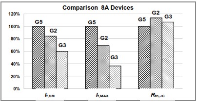
Fig. 5. Comparison of surge current capabilities (IF,MAX and IF,SM ) and thermal resistance RthJC, between SiC SBD technologies. All data taken from datasheet of the corresponding 8A devices, and referenced to G5 (ref = 100%).
In G5, the lower R can be explained by the better heat dissipation of the thin chip (Fig. 3).
In addition, thermal behavior has also an impact on the surge current capability: G5 device is
thus able to support higher current values, i.e. higher losses, before reaching the maximum
junction temperature, and its consequent destruction.
4. Experimental Results in CCM PFC
In this section, the performance of the G5 devices will be evaluated in a step-up circuit
(boost). The setup is fed by the ac means Vin=230 V and contains a power factor correction
(PFC) controller, for continuous current mode (CCM) operation. Further parameters and
component values are presented in Fig. 6.
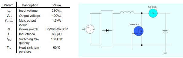
Fig. 6. CCM PFC circuit used in the experimental tests and its main parameters/component values.
Fig. 7 (a) shows the efficiency curves of the above described circuit, as a function of the output
power, from different technology generations. In Fig. 7 (b), the efficiency is normalized to
G5.
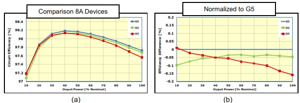
Fig. 7. Efficiency results of PFC circuit with 8A devices from G2, G3, and G5 over full output range;(parameters see Fig. 6) a) absolute values; b) normalized values to G5.
Following the schematic description in Fig. 3 it is shown that the efficiency of G5 is higher
than G2, especially at light load due to lower Q, i.e. lower switching losses. Vice versa, G5
is better than G3 is at high load conditions due to lower Vc values, i.e. lower conduction
losses. Within the three discussed generations the G5 has the lower product Qc
Paper 24 x Vf, andbecomes therefore benchmark in efficiency for the entire power range.
5. Conclusion
This paper has introduced the new family of SiC Schottky barrier diodes from Infineon Technologies,produced through a new and exclusive thin-wafer technology. The main electrical
and thermal benefits related to the thin-wafer technology have been addressed, as well as
their impact in the device performance. As demonstrated by experimental tests in a PFC circuit,
G5 offer the best balance between conduction and switching losses, offering the best
efficiency to the system, over the full load range.
6. Literature
[1] Friedrichs, P., “SiC Power Devices - Lessons Learned and Prospects After 10 Years of Commercial Availability”,
at the The International Conference on Compound Semiconductor Manufacturing
Technology 2011. Available on-line on http://gaasmantech.com/Digests/2011/papers/12b.1.pdf
[2] Bjoerk, F. et al, “2nd Generation 600V SiC Schottky Diodes Use Merged pn/Schottky Structure for
Surge Overload Protection”, APEC 2006, proceedings of.
[3] Holz, M. et al, “SiC Power Devices: Products Improvement using Diffusion Soldering”;
ICSCRM2008, proceedings of.
[4] Rupp, R. et al „Performance of a 650V SiC diode with reduced chip thickness”, ICSCRM2011, proceedings of.
[5] Holz et al, “Reliability considerations for recent Infineon SiC diode releases”, Microelectronics Reliability,2007.
[6] thinQ! TM Comparison 8A Devices Normalized to G5 SiC diodes datasheets. Available in internet: www.infineon.com/sic.


